Industrial X-ray imaging helps engineers assess solder joint void distribution, measurement repeatability, and process-related inspection questions without dismantling the package.
What BGA void inspection can show
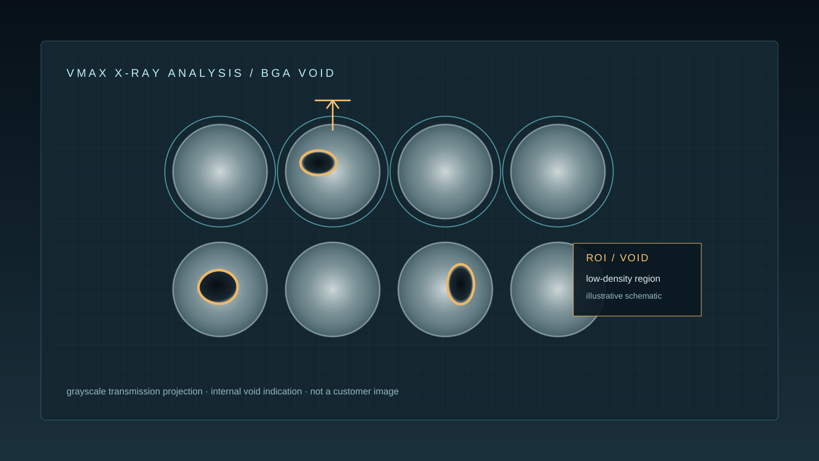
A controlled X-ray inspection workflow can reveal void location, apparent area, and distribution within hidden BGA solder joints.
- Record the imaging condition and sample orientation
- Review measurements together with package structure and process evidence
Inspection target
Hidden BGA solder joints between the package and PCB, with attention to void location, apparent area, distribution, and relation to the joint interface.
Inspection considerations
- Keep package orientation, imaging condition, and ROI rules consistent when comparing samples.
- Do not treat a dark projection area as a confirmed void without checking overlap, joint geometry, and image correction.
Measurable observations
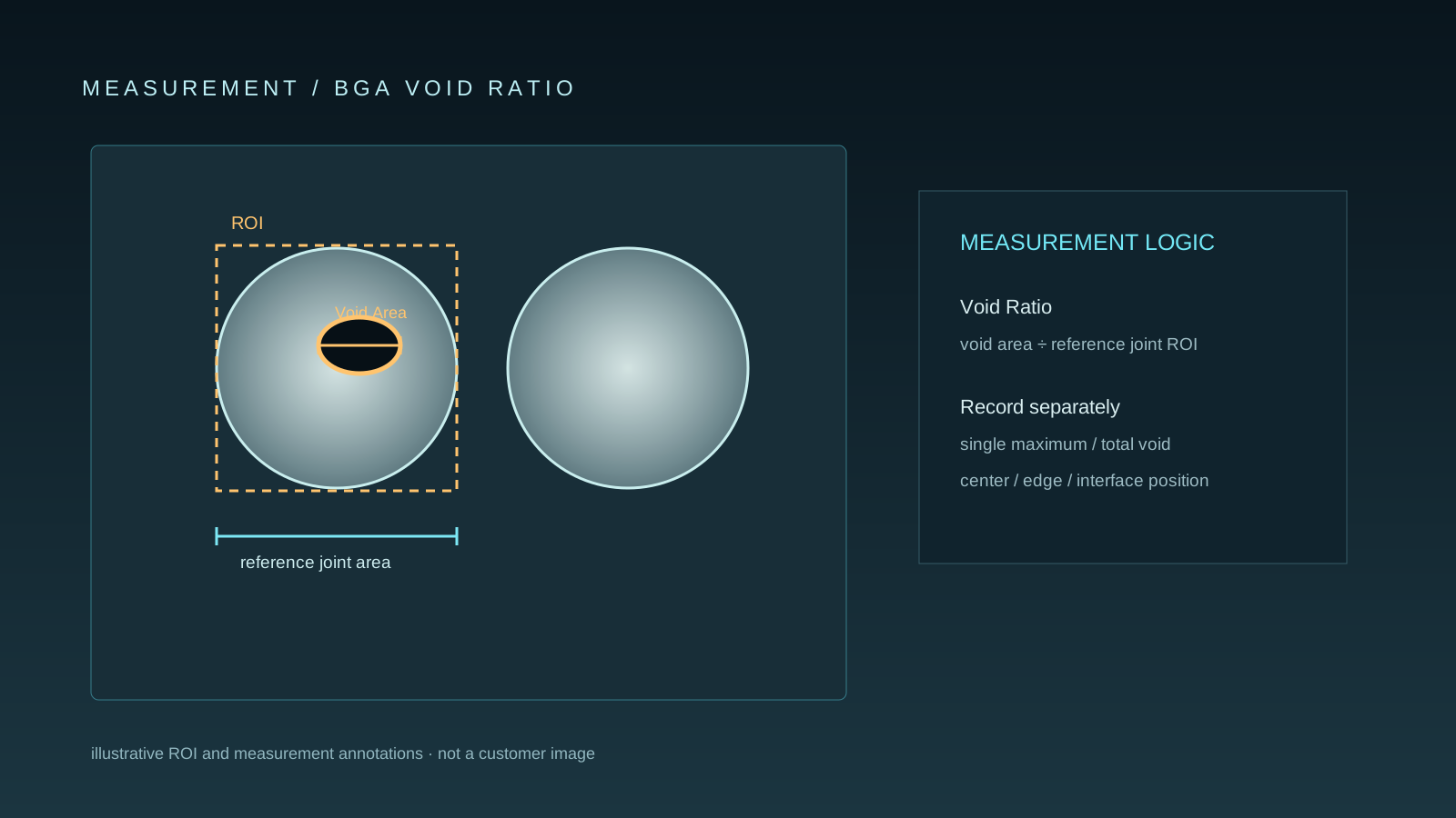
- Void area: Record the segmented projected area and the segmentation rule used.
- Void ratio: Define the joint reference area and state whether multiple voids are combined.
- Void position: Relate the indication to the joint center, pad interface, and edge.
Process and troubleshooting guidance
- Compare void results with SPI, placement, reflow, and lot information.
- Retain original images, ROI settings, and sample orientation for repeatability.
Capability boundary
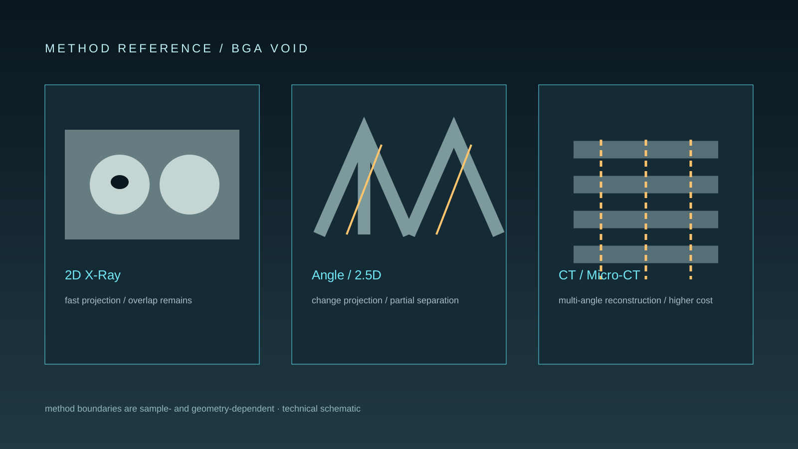
- 2D X-ray provides projection evidence and may overlap structures at different depths.
- Angle views or CT can support further review when geometry and sample attenuation permit, but imaging evidence is not a standalone process root-cause conclusion.