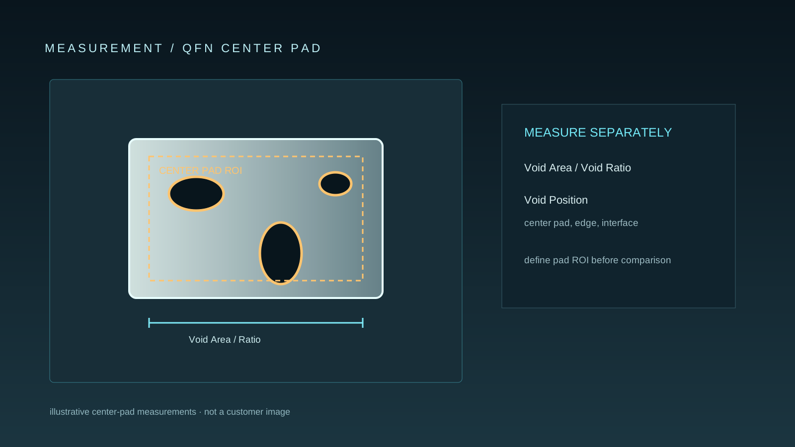
QFN void inspection focuses on hidden center-pad solder structures where optical inspection cannot directly show internal void distribution, supporting solder joint analysis.
Why QFN voids need internal inspection
X-ray image analysis can provide non-destructive evidence about apparent void area, location, and clustering within a hidden QFN solder joint.
- Separate measurement results from a universal pass threshold
- Consider package geometry, pad design, and reliability requirements
Inspection target
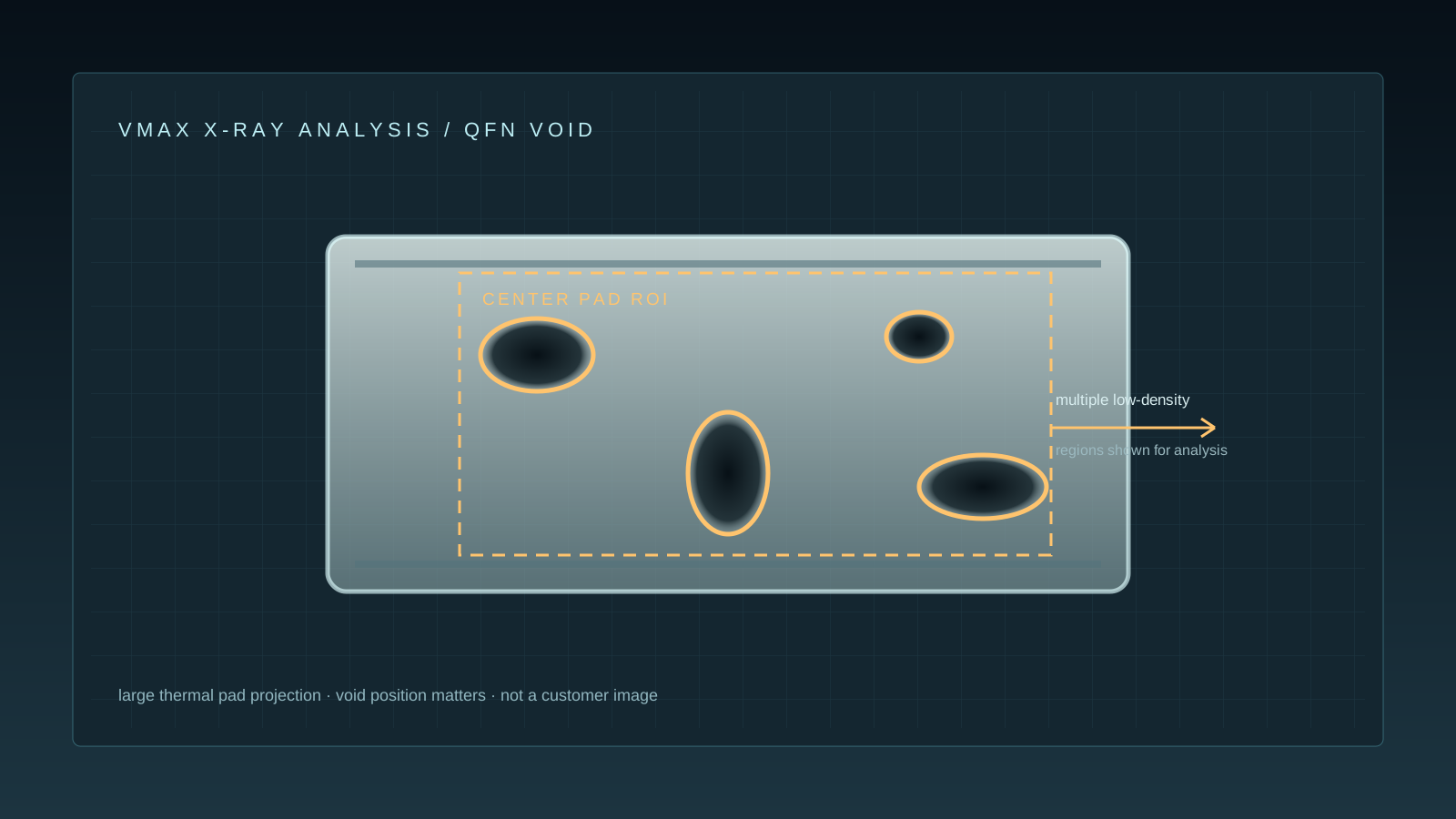
The hidden QFN center-pad and surrounding solder structures where void location, apparent area, and clustering may affect solder joint analysis.
Inspection considerations
- Keep package orientation and imaging conditions comparable across QFN samples.
- Interpret projected void area together with pad layout, package geometry, and the applicable reliability requirement.
Measurable observations
- Void area: Record apparent area within a defined center-pad ROI.
- Void location: Relate the indication to the center pad, thermal path, and joint boundary.
- Void clustering: Record whether indications are isolated or grouped within the solder region.
Process and troubleshooting guidance
- Compare image observations with stencil design, paste printing, placement, reflow, and lot records.
- Keep a universal pass threshold separate from the measurement record unless a customer specification defines it.
Capability boundary
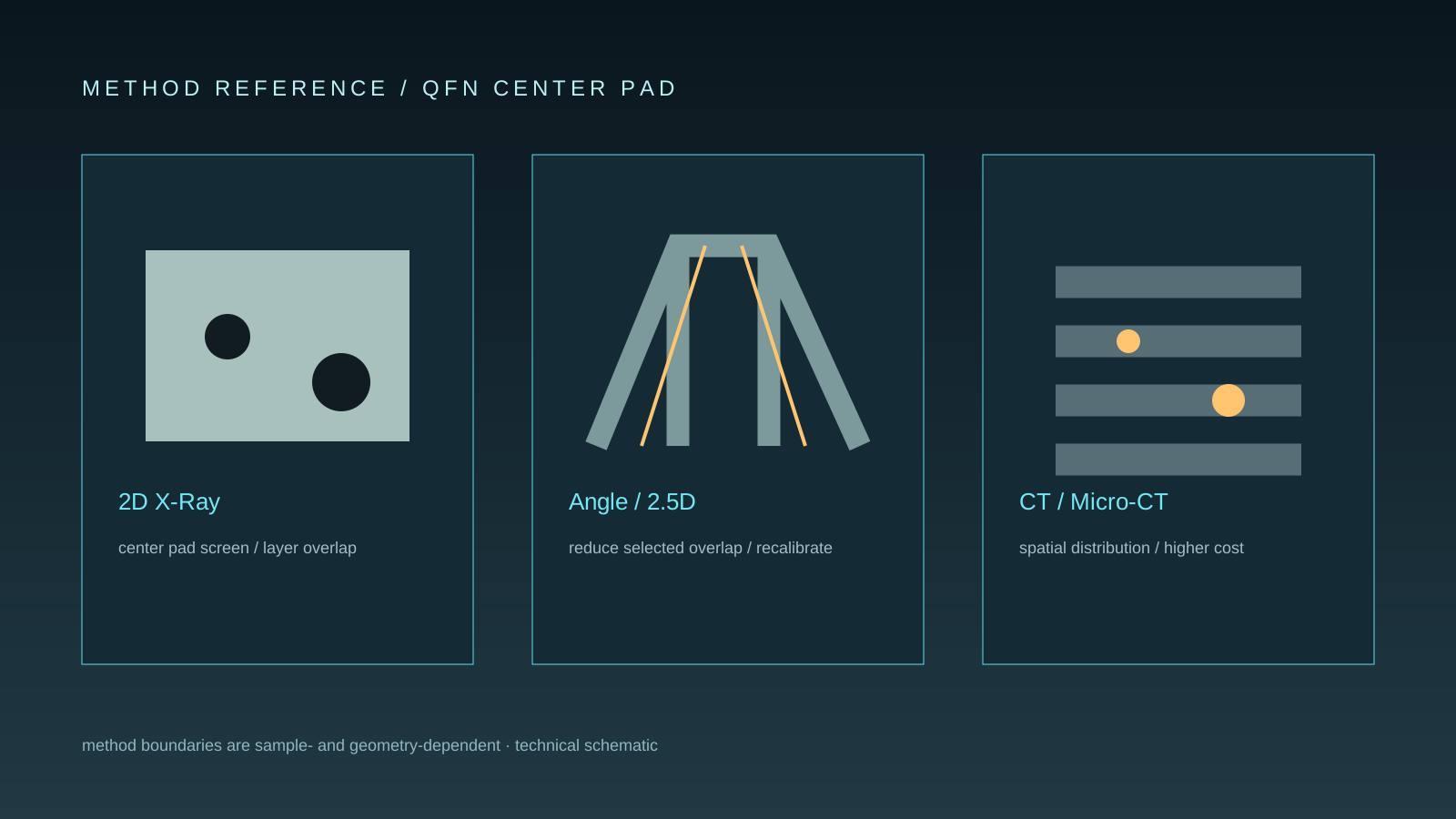
- 2D X-ray supports fast screening but cannot inherently resolve every depth relationship.
- CT or angled review may support complex cases when sample size, attenuation, and required resolution are suitable.